Question 1) Design of a switching power converter PART I
Power electronic circuits depend on digital design for their control. A boost converter is one example, where it's switching control input (S) to its NMOS transistor is a square wave of variable duty cycle (d), and ideal voltage gain of 1/(1-d). This charges up an inductor d % of the time, and then dumps the charge into an output capacitor during each off cycle - the result is a boosted voltage. You can use these for many interesting projects converting small voltages, i.e. from a battery or solar cell to power heavy loads like motors, etc. Do a quick ideal power analysis VoutIout = VinIin, and observe what happens to Iin as Vin gets very small (i.e. be careful not to burn things!!!).
The following is a schematic of a DC/DC boost converter CMOS chip deployed in an implantable device application. The circuit works by converting its small input voltage of 0.8 V max to ~2 V (Vboost) so that a CMOS transmitter has enough voltage to reliably output a wireless signal from a subcutaneous implant (under the skin of an animal). Current load, losses through the NMOS, inductor, diode, as well as an unreliable input voltage all play a role in determining the duty cycle necessary to provide 2 V output. Part I of this activity is do design the voltage control which computes this value (d) based on feedback from measurement of Vboost. Note: d is not to be confused with capital D, the input of a D flip flop.
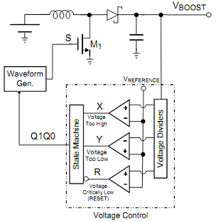
a) We designate Q1Q0 to be the state variables representing the duty cycle of the square wave activating NMOS switch M1. Note that operating at 100% duty cycle would mean S = 1 constantly and short the inductor to ground, which wouldn't allow any charge transfer to Vboost, and will probably cook the inductor! However, zero percent is desirable because when S = 0 the system can turn off and save power when not in use.
Find all values (in equally spaced intervals from 0% -- 75%) that can be realized with the 2--bit scheme. Record this in a table that lists the states to the corresponding duty cycle. Q1Q0 = 00, Q1Q0 = 11 have been filled out for you.
|
Q1Q0
|
Duty Cycle (d)
|
|
00
|
0%
|
|
01
|
|
|
10
|
|
|
11
|
75%
|
b) The voltage control block modifies the duty cycle depending on the measured Vboost. Let this measurement be reflected in logic signal X. Complete the blanks in the table for the correct X and Y inputs under each condition.
|
Input Condition
|
Voltage Control Inputs
|
Action Taken
|
|
Vboost < 1.8 V
|
R = 0
|
Increase to maximum duty cycle (asynchronous reset)
|
|
1.8 V <= Vboost < 1.9
|
R = 1, X = 0, Y = 1
|
Increase duty cycle to its next highest value
|
|
1.9 V <= Vboost < 2.1
|
R = 1, X = , Y =
|
None
|
|
Vboost > 2.1 V
|
R = 1, X = , Y =
|
Reduce duty cycle to next lowest value
|
c) Assume that a command to decrease d when at 0% produces a 0% next state, and increasing d past 75% results in 75% for the next state. Implement the sequential circuit that produces the correct Q1Q0. It is best to start with a state transition table. Fill out this table based on the information in part (b).
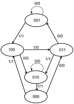
d) Draw the state machine diagram corresponding to the table from part (c).
e) Design and draw the circuit based on the information from parts (c) and (d).
f) Why was it necessary to incorporate the restrictions from part (c)? In other words, what are the practical reasons we chose to guarantee the duty cycle stays at 0% (when it's requested to reduce d) and stays at 75% (when requested to increase d)?
Question 2) Design of a switching power converter PART II
Now we have the design that computes the correct duty cycle in the format Q1Q0 which represents 0% to 75%. We can set these state variables equal to d1d0 and consider them inputs to our next circuit, which generates (S) controlling the NMOS. For example, if d = 75%, then S is logic '1' 75% of the time and '0' 25% of the time. The idea behind this design is to generate a 2--bit up counter (C1C0) with output S = 1 if d1d0 > C1C0 and S = 0 if d1d2 <= C1C0.
a) Design the 2-bit counter circuit that cycles c1c0 = 00, 01, 10, 11 and loops back to 00, with inputs d1d0 and output S. Show the state transition table.
b) Show the state machine diagram.
c) Derive the logical functional expressions, and logic circuit.
d) Draw the timing diagrams for S for both 25% and 75% duty cycles. At minimum, these should have the CLK for the 2-bit counter, C1, C0 and S.
e) Analog engineers designing the clock for the 2-bit counter determined due to constraints in their power budget, the maximum frequency of their clock will be 1 MHz because as clock frequency increases, the clock consumes more power. What would be the maximum switching frequency of the converter (signal S)? Propose a general rule for obtaining the converter's switching frequency based on: the counter's clock frequency and # of bits of the counter.
f) Explain the design tradeoff between duty cycle precision (# of bits), and maximum clock frequency. Why would in some applications it be preferable to have less precise duty cycles?
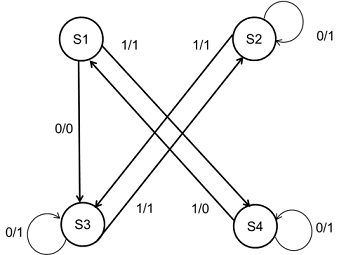
Question 3) A sequential circuit has one input and one output
The state diagram is as shown. Design the sequential circuit with (a) T flip--flops, (c) JK flip flops
Question 4) State machine minimization
It is desirable to implement a state machine with the minimum number of states. This is accomplished by merging equivalent states. Two states are equivalent if and only if, for any input, the two states have identical outputs and the corresponding next states are equivalent. Minimize the state machine in the figure and draw the minimized machine.
Question 5) Design a sequential circuit with 2 flip--flops and one input X
When X = 1, the flip flop outputs repeat the sequence 00, 01, 10. When X = 0, they repeat the sequence 11, 10, 01. Design the circuit with a) D flip-flops and b) T-flip flops. Show all work: state machine diagrams, tables, k-maps, etc.