Ask Question, Ask an Expert

+61-413 786 465

info@mywordsolution.com

Ask Electrical & Electronics Expert

1. (a) Name the three major groups of contamination and briefly describe their physical characteristics.

(b) Where do the above contamination types come from? Give one example of each.

2. Name two processes metrics which would be worsened by poor cleanroom practices in a semiconductor cleanroom. Describe briefly what is meant by each term.

3. (a) What sizes of particles would cause problems for the following processes:

- 5 μm bipolar

- 4.5 μm NMOS

- 1.1 μm CMOS

- 0.9 μm BICMOS

- 0.3 μm CMOS?

(c) What effect is illustrated by the above?

(d) What additional particle related issue affects smaller feature size processes?

4. FIGURE 1 shows a system which is to be assessed for particles. The maximum specification limit on the system is +100 particles of >0.5 μm.

(a) A CWC is run by processing a test wafer through the entire sequence (process module 1 and module 2) and it reveals that 350 particles of >0.5 μm have been added. Comment on this finding.

(b) A second CWC is run with the wafer being processed only through module 1 and it reveals that 334 particles of >0.5 μm have been added. Comment on this finding.

(c) A third CWC is run with the wafer being processed through module 2 and it reveals that 328 particles of >0.5 μm have been added. Comment on this finding.

(d) Suggest where the particles may be coming from and suggest ways to isolate the sources of particles.
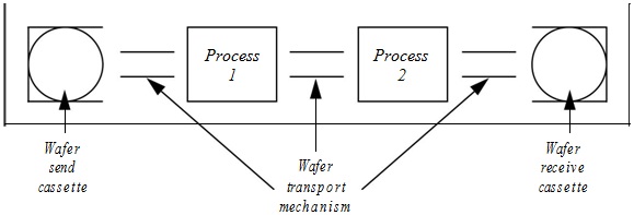
113_Top view.jpg

FIG. 1

5. The approximate number, N, of square chips of area A that can be formed on a wafer of diameter D is given by the equation:

N ≈ π/4A.(D - √A)2

A VLSI chip is to be fabricated on a 300 mm wafer and uses 6 lithography processes. It is reckoned that on average there will be 2 defects per wafer for each lithographic process. Assume the defects fall on different chips.

Calculate the cumulative percentage yield of the lithography processes if the chip has an area of:

(a) 0.5 cm2

(b) 1 cm2

(c) 2 cm2

(d) 4 cm2.

Comment on the results.

6. In the production of a CMOS gate the required doping may be achieved by thermal diffusion or by ion implantation.

Briefly describe each process and the relative advantages of each.

Identify which process is used in the various doping stages in the production of a CMOS gate.

Explain the effect upon doping methods as feature sizes in modern devices fall to well below the sub- micron feature size.

Electrical & Electronics, Engineering

  • Category:- Electrical & Electronics
  • Reference No.:- M93110177
  • Price:- $65

Guranteed 36 Hours Delivery, In Price:- $65

Have any Question? 


Related Questions in Electrical & Electronics

Advanced computational techniques in engineering assignment

Advanced Computational Techniques in Engineering Assignment - Optimisation For this assignment, you are required to carry out the process of attempting to solve different optimisation problems. For each question, you are ...

Case studythis assignment consists of a written report of

CASE STUDY This assignment consists of a written report of approximately 1000 words and any diagrams in which you are asked to critically compare different process methods used to achieve the same result and show an awar ...

Questions -problem 1 - determine the laplace transform ofa

Questions - Problem 1 - Determine the Laplace transform of: (a) cos(ωt + θ) (b) sin(ωt + θ) Problem 2 - Obtain the Laplace transform of each of the following functions: (a) e -2t cos(3t)u(t) (b) e -2t sin(4t)u(t) (c) e - ...

Nanotechnology engineering - resonance circuits questions

Nanotechnology Engineering - Resonance Circuits Questions - Q1) A series RLC network has R = 2KΩ, L = 40mH and C = 1μF. Calculate the impedance at resonance and at one-fourth, one-half, twice, and four times the resonant ...

Discuss the role of load factor on the cost of electrical

Discuss the role of load factor on the cost of electrical energy.

Question 1 in the voltage regulator circuit in figure p221

Question 1: In the voltage regulator circuit in Figure P2.21, V 1 = 20 V, V Z = 10 V, R i = 222Ω and P z (max) = 400 mW. (a) Determine I L, I z , and I L , if R L = 380Ω. (b) Determine the value of R L , that will establ ...

Question 1 - for the transistor in the circuit shown in

Question 1 - For the transistor in the circuit shown in Figure, assume β = 120. Design the circuit such that I CQ = 0.15 mA and R TH = 200kΩ. What is the value of V CEQ ? Question 2 - (a) For the circuit shown in figure, ...

Questions -q1 a single-phase transformer rated 21 kv130 v

Questions - Q1. A single-phase transformer rated 2.1 kV/130 V, 7.8 kVA has the following winding parameters: r1= 0.7Ω, x1 = 0.9Ω, r2 = 0.04Ω and x2 = 0.05Ω. Determine: a. The combined winding resistance ________ Ω and le ...

Summative assessmentin 2017 sej101 assessment will consist

Summative Assessment In 2017 SEJ101 assessment will consist of nine tasks that will develop a portfolio of your assessed work. Throughout the trimester you will have the opportunity for feedback on all nine tasks before ...

Problem 1given a sequence xn for 0lenle3 where x0 1 x1 1

Problem # 1: Given a sequence x(n) for 0≤n≤3, where x(0) = 1, x(1) = 1, x(2) = -1, and x(3) = 0, compute its DFT X(k). (Use DFT formula, don't use MATLAB function) Problem # 2: Use inverse DFT and apply it on the Fourier ...

  • 4,153,160 Questions Asked
  • 13,132 Experts
  • 2,558,936 Questions Answered

Ask Experts for help!!

Looking for Assignment Help?

Start excelling in your Courses, Get help with Assignment

Write us your full requirement for evaluation and you will receive response within 20 minutes turnaround time.

Ask Now Help with Problems, Get a Best Answer

Why might a bank avoid the use of interest rate swaps even

Why might a bank avoid the use of interest rate swaps, even when the institution is exposed to significant interest rate

Describe the difference between zero coupon bonds and

Describe the difference between zero coupon bonds and coupon bonds. Under what conditions will a coupon bond sell at a p

Compute the present value of an annuity of 880 per year

Compute the present value of an annuity of $ 880 per year for 16 years, given a discount rate of 6 percent per annum. As

Compute the present value of an 1150 payment made in ten

Compute the present value of an $1,150 payment made in ten years when the discount rate is 12 percent. (Do not round int

Compute the present value of an annuity of 699 per year

Compute the present value of an annuity of $ 699 per year for 19 years, given a discount rate of 6 percent per annum. As