Ask Question, Ask an Expert

+61-413 786 465

info@mywordsolution.com

Ask Electrical & Electronics Expert

Design work involves producing layouts for circuit in Fig. 1. Such layouts correspond to the patterns developed on the masks, for use in the fabrication process, as discussed in lectures. Each of the layouts MUST be drawn on a graph paper with stipulated scale (e.g. 1pm per cm). The four masks that need to be defined are: device area, gate stripe, contacts and metal pattern. Produce individual layouts for each device i.e. A, B, C and RL, and also the overall layout for the circuit, in terms of the minimum feature size. Make sure to include the alignment errors between the layouts and minimise the area used.

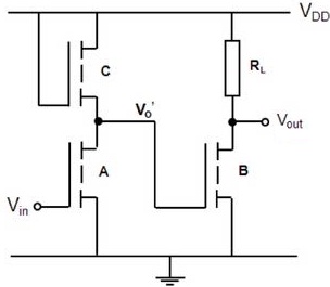
Description: The circuit in Fig. 1 consists of a two-stage inverter, where the output from the 1st inverter Vo' is fed into the input gate of the 2nd inverter. The driver of both inverters consists of enhancement type n-MOS transistors A and B. Note these transistors have identical aspect ratios. It can be assumed that the threshold voltage VT to be 0.3 V. For the loads, the 1st inverter has an (active) saturated n-MOS transistor C, whilst the 2nd inverter has an (passive) implanted resistor load RL. Note the resistance value of C is equal to the resistance RL, and similarly, the resistance of A is identical to the resistance of B, when the transistors are on.

870_Two-stage inverter.jpg

For your design, calculate the dimension of the channel width W for the drivers and respective dimensions of W and L for C and RL. To assist you with the calculation, you can select appropriate value for the output voltage Vo, which corresponds to the logic 0 condition, assuming a logic 1 input to be equal to VDD = 5 V. Note the value of Vo needs to be lower than VT of the driver B in order to ensure that the transistor remains off at logic 0. The value depends on the ratio of the resistances between the driver and load for each inverter. Also for the implanted resistor RL, you can assume a sheet resistance of 150Ω/square, where each square is defined by minimum feature size.

Note for the layouts you must take account the alignment accuracy λa, which can also be assumed to be equal to the minimum feature size. For your calculation, you can assume the following values for the parameters:

i. Minimum feature size λm = 0.5 μm

ii. Supply voltage VDD = 5V (Logic 1 input)

iii. Threshold voltage VT = 0.3 V

iv. Sheet resistance 150 Ω/square

v. Device constant is given as,

β = (μCo)W/L = (βo)W/L                 where βo = 1.8 x10⁻⁴ AV-2

Useful hints:

1. If driver A is on and Vo,' is small then the current through A can be approximated as,

ID = βA[(Vin - VT)Vo' - Vo'2] ≈ βA[Vin - VT)]

With the aid of this current expression and Ohms law, the value of the resistances for driver A and load C can be determined. The aspect ratio of the load C can be obtained using the saturation current (note this load always operates in saturation regime) as,

ID = βc/2(VDD - VT)2.

2. The resistance values for the two loads are the same i.e. Rc = RL. To determine their dimensions i.e. L and W, of the implanted resistor RL. use the given the sheet resistance and consequently calculate the number of squares required. For C, determine the value of W and L accordingly. Note this W/L is not the same as W/L for A or B.

For the Report: Give a brief description of the circuit operation in Figure 1. Include all your calculations and reasons for the assumptions made. Represent all respective individual and overall design layouts in scaled graph paper, in terms of minimum feature size. Use different shading to indicate the different regions and include the alignment errors between respective layouts.

Electrical & Electronics, Engineering

  • Category:- Electrical & Electronics
  • Reference No.:- M92273682
  • Price:- $60

Guranteed 36 Hours Delivery, In Price:- $60

Have any Question?


Related Questions in Electrical & Electronics

Assignment -problem 1 -a consider the simplified dc system

Assignment - Problem 1 - a) Consider the simplified dc system shown in Fig. 1. Only one converter is modeled, with the remote end represented by a dc source. The ac system is rated at 345 kV, with the converter transform ...

1 a name the three major groups of contamination and

1. (a) Name the three major groups of contamination and briefly describe their physical characteristics. (b) Where do the above contamination types come from? Give one example of each. 2. Name two processes metrics which ...

1 goalin this project you will solve a non-trivial design

1 Goal In this project you will solve a non-trivial design problem explicitly using the divide-and-conquer (D&C) approach. The main reason for using the D&C approach is the ease of the design process and the streamlined ...

Questions -q1 a single-phase transformer rated 21 kv130 v

Questions - Q1. A single-phase transformer rated 2.1 kV/130 V, 7.8 kVA has the following winding parameters: r1= 0.7Ω, x1 = 0.9Ω, r2 = 0.04Ω and x2 = 0.05Ω. Determine: a. The combined winding resistance ________ Ω and le ...

Question -i a star-connected three-phase synchronous

Question - (i) A star-connected, three-phase synchronous induction motor takes a current of 10 amps from a 415 volt supply at unity power factor when supplying a steady load. If the synchronous reactance is 5 ohms/phase ...

Research report1 read 3 to 4 journal articles about digital

Research report 1. Read 3 to 4 journal articles about digital control or industrial control, eg. one particular application, implementation aspect such as selection of sampling time, hardware etc. No text book example is ...

Assignment - power distribution system transformerscomplete

Assignment - Power Distribution System Transformers Complete your calculations, drawings, and answers, neatly handwritten on these sheets and hand in at the start of lecture in week 6. Absolutely no late submissions will ...

Problem 1given a sequence xn for 0lenle3 where x0 1 x1 1

Problem # 1: Given a sequence x(n) for 0≤n≤3, where x(0) = 1, x(1) = 1, x(2) = -1, and x(3) = 0, compute its DFT X(k). (Use DFT formula, don't use MATLAB function) Problem # 2: Use inverse DFT and apply it on the Fourier ...

Questions -problem 1 - determine the laplace transform ofa

Questions - Problem 1 - Determine the Laplace transform of: (a) cos(ωt + θ) (b) sin(ωt + θ) Problem 2 - Obtain the Laplace transform of each of the following functions: (a) e -2t cos(3t)u(t) (b) e -2t sin(4t)u(t) (c) e - ...

Questions -problem 1 - given the sinuosidal voltage vt 50

Questions - Problem 1 - Given the sinuosidal voltage v(t) = 50 cos(30t+10 o ) V, find: (a) the amplitude V m (b) the period T, (c) the frequency f and (d) v(t) at t = 10 ms. Problem 2 - A current source in a linear circu ...

  • 4,153,160 Questions Asked
  • 13,132 Experts
  • 2,558,936 Questions Answered

Ask Experts for help!!

Looking for Assignment Help?

Start excelling in your Courses, Get help with Assignment

Write us your full requirement for evaluation and you will receive response within 20 minutes turnaround time.

Ask Now Help with Problems, Get a Best Answer

Why might a bank avoid the use of interest rate swaps even

Why might a bank avoid the use of interest rate swaps, even when the institution is exposed to significant interest rate

Describe the difference between zero coupon bonds and

Describe the difference between zero coupon bonds and coupon bonds. Under what conditions will a coupon bond sell at a p

Compute the present value of an annuity of 880 per year

Compute the present value of an annuity of $ 880 per year for 16 years, given a discount rate of 6 percent per annum. As

Compute the present value of an 1150 payment made in ten

Compute the present value of an $1,150 payment made in ten years when the discount rate is 12 percent. (Do not round int

Compute the present value of an annuity of 699 per year

Compute the present value of an annuity of $ 699 per year for 19 years, given a discount rate of 6 percent per annum. As