VLSI System Design & Modeling Technique Design Laboratory
1. Objective
These two lab experiments are designed to complement the theoretical knowledge acquired from the lectures with practical skills on how to design, verify, and implement complex VLSI systems using VHDL.
In the first lab the students will be exposed to an industry standard CPLD/FPGA design environment - Quartus II from Altera. They will be briefed on how to use the software to implement their design. In the second lab, the students will be taught to synthesize their codes using Quartus II and then finally download the codes on the Altera University Board depends on the designed project given.
The overall objective is to prepare the students for the lab assignments and course project, which will be explained in section 3 and 4 of this document respectively. The labs themselves will not be graded but attendance to the labs is compulsory so the students will be able to learn how to use the tools to do their project. The lab assignments count for 10% of the total grade and course project counts for 20% of the total grade.
2. Introduction
In this lab, there are two sections; lab assignments and project. Students are asked to write the VHDL codes for few circuits for the lab assignments. Students are then required to do the assigned tasks for their project. Detailed procedures on how to design a circuit are not given in the lab sheet. Students have to use their creativity in completing the task. This will also sharpen students' skills, as engineers are not procedure-followers. An introduction session will be held to get students acquaintance to the Quartus II software.
3. Lab assignments
The lab assignments (Date of submission: week 9th) must be done by individuals (no groups). The assignments are as follow:
Session 1:
Q1. a) Create the truth table of a half adder.
b) Compute the simplified output signal equations of the half adder.
c) Model the half adder using VHDL.
d) Perform the functional verification and performance analysis of the half adder that you modeled in part (c).
Q2. a) Create the truth table of the full adder.
b) Compute the simplified output signal equations of the full adder.
c) Model the full adder in VHDL using the equations that you computed in part (b).
d) Model the full adder in structural VHDL using component declaration (half adder).
e) Model the full adder in VHDL using the package function "+".
f) Perform the functional verification and performance comparison between the full adders that you modeled in previous parts.
Session 2: Combinatorial circuits
a) Model a 8-to-1 multiplexer in VHDL
b) Create a test-bench to test circuit in (a)
Session 2: Sequential circuits
a) Synchronous DFF with asynchronous reset
b) Synchronous BCD counter
After mastering the software with above assignments, by using Quartus II, the students will be required to design, simulate and verify the functionalities of a relatively complex digital system, then synthesize the codes.
4. Course Project
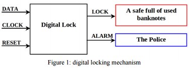
Design a three-input, two-output sequential digital circuit which functions as a digital locking mechanism. Design diagram is shown in Figure 1.
If a logic level 0 appears on the LOCK output then the safe is unlocked. If a logic level 1 appears on the ALARM line then the police are summoned. When a logic 1 appears on the RESET line, the mechanism is put into the known "reset" state in which the LOCK output is set to logic level 1 (locked). In this state the lock mechanism is waiting for a specific five binary digit sequence of 1s and 0s to appear, one binary digit for each CLOCK pulse. If the correct sequence of digits is sent then the LOCK output becomes logic 0 and the safe opens. The safe remains open as long as the DATA input line is at logic 1. When logic 0 appears on the DATA input the system returns to the reset state. If a wrong sequence of digits is input then the ALARM output signal becomes a logic 1 and it remains so for any sequence of values appearing at the DATA input. The only way to remove the Alarm signal is to set the RESET input line to 1.
5. Report for Project
After completing the chosen design task, a project report should be submitted by each group. In this report, all the design decisions must be justified. All relevant information must be provided. Organization, conciseness, and completeness are of paramount importance. The following information must be included:
(a) Theory of operation
(b) The block diagram, state diagram, truth table.
(c) Functional explanation of the design
(d) Source codes
(e) Expected results (testbenches)
(f) Simulation results (waveform)
(g) Synthesis - Technology view and RTL view
(h) Conclusions
(i) Citation to references is another vital part of the report. All referred materials/articles must be properly cited.
Attachment:- Assignment File.rar