Topics
• Background:
• No questions explicitly on 321 material, but you are expected to understand basic characteristics and DC analysis techniques for MOSFETs and BJTs. For example: regions of operation, MOSFET I-V and gm equations, 4-resistor DC bias circuit.
• Chapter 13: all sections except 13.4
• Be able to construct DC and ac circuit
• Be able to find small-signal parameters for BJT and MOS
• Be able to draw hybrid-pi model and calculate Av, Rin and Rout for CE and CS amplifiers
• Chapter 14: sections 14.1 - 14.5, 14.8 - 9
• Be able to recognize the 6 amplifier configurations: CE, CS, CC, CD, CB, CG
• Be able to calculate Av, Rin and Rout for all - won't need to derive
• CE/CS could have RE/RS bypassed or not
• Understand the characteristics of each, be able to compare advantages and disadvantages, be able to choose which configuration best suits a given set of specifications
• Be able to design an amplifier circuit to meet certain specifications (simple)
• Be able to calculate characteristics for simple multi-stage combinations
• Chapter 15: section 15.1 only
• Understand differential and common-mode operation
• Be able to calculate: Ad and Ac for differential or single output, CMRR, Rid, Ric, Rout
• Be able to design a differential amplifier circuit to meet certain specifications (simple)
• End of chapter summaries are good reviews of the main concepts!
Practice problems
1. Design the differential amplifier in Figure 15.13 (a) using IC = 500 μA. The specifications are |Ad_single| = 200 and CMRR = 1000. This is a rough design, so you can use approximations such as α ~ 1 and ro ~ ∞. There is no RI or R3. Find the following to satisfy the design specifications:
(i) IEE, (ii) RC, (iii) Ac_single and (iv) REE.
2. A common-emitter amplifier is shown below. The BJT has β = 80 and VA = 80 V. The dashed lines on C3 mean the capacitor is in the circuit in part of this problem and not in the circuit in another part. Assume: VT = 25 mV, VBE = 0.7 V, the capacitors are all large and Vi is a small-signal, mid-band ac source. All resistors are in Ω (i.e., 10k = 10 kΩ .)
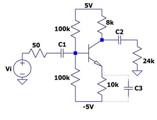
a) Calculate the DC operating point, IC and VCE
b) Calculate gm, rΠand ro
c) Draw the ac circuit for the amplifier, including the small-signal model of the transistor, for the following two cases: (i) capacitor C3 is in the circuit and (ii) capacitor C3 is not in the circuit.
d) Calculate Av, Rin and the approximate Rout for case (i) and for case
3. Fill in the table below with "high" or "low", understanding that these are relative comparisons. From what we've seen, for gain, "high" could be anything from around 5 - 200. "Low" means ≤ 1. For resistance, "high" typically means kΩ up to MΩ , while "low" would be less than a kΩ or so. These are typical numbers we see, not an absolute rule.
|
|
Rin
|
Rout
|
Av
|
|
CS/CE
|
|
|
|
|
CG/CB
|
|
|
|
|
CD/CC
|
|
|
|
4. A voltage amplifier is required to have Av = 40 dB, Rin = 50 kΩ and Rout = 100 Ω . Could this be designed with a single stage? Which configuration(s) would you use?
5. A transresistance amplifier has current input and voltage output. The transresistance gain is Ar = vo/is. A small-signal model of a "generic" transresistance amplifier is shown below (i.e., the transistor could be either a BJT or a MOSFET.) The parameter Kr is the transresistance in Ω , comparable to gm.
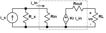
a) Derive expressions for (i) the terminal gain Art = vo/iin and (ii) the overall gain Ar = vo/is.
b) For this type of amplifier, do you want Rout to be large or small? Explain why.
c) For this type of amplifier, do you want Rin to be large or small? Explain why.
6. A 2-stage voltage amplifier is shown below. The capacitor C2 is the connection between the two stages. Answer part c) in terms of the resistors as labeled in the figure, and the transistor small-signal parameters such as rΠ1 or gm2. Use RB1 = R1||R2 and RB2 = R3||R4; any other equivalent resistances such as RL or RTh need to be defined. You can neglect ro in this problem.
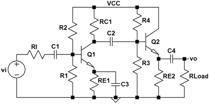
a) What is the configuration of the first stage, CE, CC, or CB?
b) What is the configuration of second stage, CE, CC, or CB?
c) Write expressions for the following: the input resistance of the amplifier, the output resistance of the amplifier, the gain of the first stage (assume you can neglect RI), the gain of the second stage.
d) Would this configuration make a good voltage amplifier? Explain why or why not.