Problem 1) (part "a") Consider the circuit above on the left (often used for Neural recording).
a. Assuming an ideal op-amp, write the transfer function, H(s)=Vout(s)/Vin(s) of the amplifier, in terms of C1, C2, and RF. Choose C1, C2 and RF so that: the lower 3dB cutoff is 10Hz, the flat-band gain is -100 (40dB), and the largest capacitance is 20pF (Note, RF will be very large).
b. Now, If the opamp is a real op-amp with finite gain Ao=10,000, (for now assuming ro=0) but you use the same values for RF, C1 and C2 how do the gain and high-pass corner frequency change?
c. What is the DC level of the output?
d. Assume the op-amp has an input-referred noise of 100nV/Hz½ and that RF generates thermal noise (but ro does not). Solve for the output and input referred noise of the amplifier as a whole, as a function of frequency. And sketch the input referred noise on a Bode plot.
e. What is the transfer function if you assume that the op-amp is actually a trans conductance gm, with output impedance ro, and load CL (write in terms of gm, ro, CL, RF, C1 and C2)? Write out KCL, but before solving lots of nasty algebra, assume that ro << RF, gmro >> C1/C2, and CL >> C2 and neglect terms appropriately. (Hint: What is your effective Ao(ω) now?)
f. Assuming gm=2mS, ro=5MΩ, Choose CL to set an upper-limit 3dB bandwidth of 50 kHz and compute the in-band gain.
Beyond here is Part "b"
g. Process variation: Assuming RF varies across process with a standard deviation of σR/R=4%, similarly, σC/C=3%, also assume the op-am has a finite gain of Av=gmro=10,000 and σAv/Av=10%. What is the 3-6 variation in mid-band gain? In the high-pass corner? In the low-pass corner?
h. Component matching: Assume C1 and C2 are created out of sets of 25fF unit capacitors. Assume the matching between nominally identical unit capacitors is σ(Ca-Cb)/C =1.4%. What then, are the 3-σ limits on gain?
Problem 2) Now we will design an OTA for the circuit in part 1. Start with the folded-cascode amplifier shown above. Initially, assume all transistors are sized and biased to have the same VOD=0.2V. VTHN=0.6V, VTHP=0.5V Ibias=25μA, VDD=2.5V, R=12kΩ. You may also assume that the unit NFET has W/L = 5um/1um, and unit PFET has W/L = 20um/1um.
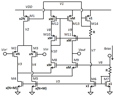
a. Compute the bias current of each transistor (M1-14) and the bias voltage of each node (V1-V10). Your answers should be in terms of M and N, Assume Vin+ = Vin = Vincm.
b. Identify sub-circuits: specifically, with transistors are part of the following circuits: differential pair, passive current mirror, active current mirror, cascode.
c. What is the minimum VDD that will still keep all transistors in saturation (assuming Vin+, and Vin- are chosen properly), give an equation in terms of VOD, VTH, and a number.
d. For VDD=2.5V, what is the range of Vincm that keeps all transistors in saturation? What is the range of Vout that keeps all transistors in saturation? For each, give an equation in terms of VOD, VTH, and a number.
e. If Vin+ increases by AV and Vin- decreases by ΔV which transistors' drain currents will increase significantly, and by how much? Which will decrease? Which will stay essentially the same? Similarly, identify which nodes are "active" (changing voltage in response to a change on the input.
For the following, questions, give your answers in terms of the unit gm and ro, of unit FETS (assuming N- and P-fets are the same in this respect), and the component counts N and M. Also provide a numerical result: assume ro=200/gm.
f. What is the approximate DC gain of this circuit?
g. What is the output resistance?
h. What is the total current consumption of the circuit?
i. What is the resistance and capacitance of each node? Assume CGD=0, CDB=CSB=CGS/4. Also assume Cgs = 20fF for unit NFETs and 80fF for unit PFETs. (You need only be accurate to ~10%)
j. Assuming CL=5pF, what is the dominant pole frequency. What are the other poles of the circuit? In each case also state which nodes(s) set that pole.
k. Assuming CL from (j) what is the unity-gain Bandwidth of the amplifier?
I. Assuming CL from (j), if the amplifier were hooked up in unity-gain feedback, what would it's phase margin be?
m. Assuming CL from (j) What is the slew rate of the amplifier?
Noise and variation.
n. Which components can you neglect when analyzing noise? Why?
o. What is the input referred noise, in terms of gm, ro, N, M, and the drain-current noise of each relevant transistor.
p. Compute the input-referred thermal noise integrated from 10Hz to 100kHz, assuming Y= 1.
q. Now, consider flicker noise, and assume the following model:
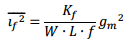
Assume Kfp=2.10-9V2(μm)2, KfN= 2.10-10V2 (μm)2
What is the total integrated flicker noise from 10Hz to 100kHz? (Hint, first find the integrated flicker noise for a unit NFET and PFET)
r. Choose N and M (integer values) to achieve an input referred noise, of approximately 100 while minimizing DC current consumption.
Beyond here is part "b"
s. Assume all transistors follow square law behavior with channel length modulation, such that:
ID = μcox (W/2L) (VTH - VGS)2(1 + VDSλ)
Also assume all devices are subject to the following process variations: σcox/cox = 5%, σλ/λ=5%, (assume cox and λ are the same for N- and P-FETs, so they "track") σVTHIN=20mV, σVTHP=20mV. Assume all other parameters are perfectly controlled. For a fixed Ibias, in a unit transistor, what 3-sigma variation do you expect in gm? In Vgs? In ro? In Cgs?
t. For the same parameters as in (s), estimate 3-sigma process variation of the amplifier's DC gain and unity-gain bandwidth (assuming CL and Ibias are constant). (Start from your results from parts f and j)
u. What is the 3-sigma variation the 2nd and 3rd most dominant poles. Given this variation relative to the unity gain bandwidth, is this enough to significantly affect phase margin?
v. To be sure of proper operation across a 3-sigma tolerance (again from (s)), what is the input common mode range of the amplifier (this is basically just a function of VTHN and VTHP)
w. Assume component-to-component mismatch is primarily in VTH, and assume each transistor varies independently as: σVTH=10mV/(WL)½. What is the 3-sigma VTH mismatch between a pair of unit NFETS? PFETS?
x. When estimating input-referred DC-offset due to VTH mismatch, which transistors can you ignore, and why?
y. What input- referred 3-sigma DC offset do you expect for N=M=1? For the values of M, N you found in part (r)?
z. Adjust W/L for better performance: As you know, decreasing VOD, for the same current, increases gm (until about when VOD<100mV, when it starts to enter sub threshold), and vice versa. Furthermore, this adjustment in bias point can be achieved just by changing W/L. Based on the above analysis, if you wanted to further reduce noise by redesigning some of the transistors to be in sub threshold, and others to have a high VOD (say 400mV). Which transistors would you bias close to sub threshold? Which would you bias at 400mV? Why?
Attachment:- Assignment File.rar